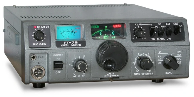
Solid state 80, 40, 20, 15 and 10-meter transceiver for fixed and mobile CW/SSB (50 Watts power output) and AM (12 Watts) operations. Single conversion receiver, good sensitivity and selectivity, CW audio filter. The VFO frequency is 5–5.5 MHz so that the receiver covers the 80-meter band directly. The VFO output is mixed with appropriate crystal oscillator for the other bands. Ideated in Japan, year of introduction 1979.
Reference market : amateur-radio
FT-7B specifications
| General |
| Frequency coverage | |
|---|---|
| Receive [1] | 3.5000 ~ 4.0000 MHz
7.0000 ~ 7.5000 MHz 14.0000 ~ 14.5000 MHz 21.0000 ~ 21.5000 MHz 28.0000 ~ 28.5000 MHz 28.5000 ~ 29.0000 MHz 29.0000 ~ 29.5000 MHz 29.5000 ~ 29.9000 MHz |
| Transmit [1] | 3.5000 ~ 4.0000 MHz
7.0000 ~ 7.5000 MHz 14.0000 ~ 14.5000 MHz 21.0000 ~ 21.5000 MHz 28.0000 ~ 28.5000 MHz 28.5000 ~ 29.0000 MHz 29.0000 ~ 29.5000 MHz 29.5000 ~ 29.9000 MHz |
| Mode | |
| CW / LSB / USB / AM | |
| Receiver |
| Sensitivity | |
|---|---|
| 0.25 uV (10dB S/N) | |
| Selectivity | |
| 2.4 kHz (-6dB)
4.0 kHz (-60dB) |
|
| RF attenuator | |
| 20dB | |
| Image rejection | |
| > 50dB (10-meter band)
> 60dB (80 to 15-meter bands) |
|
| IF rejection | |
| > 50dB | |
| NB (Noise Blanker) | |
| Yes | |
| RIT (Receiver Incremental Tuning) | |
| ± 2 kHz | |
| Frequency stability | |
| ± 300Hz max from a cold start
± 100Hz max over a 30' period after warm-up |
|
| IF (Intermediate Frequency) | |
| 1° | 9 MHz |
| CW features | |
| Semi break-in
Audio peak filter (80Hz bandwidth @ -6dB) |
|
| Transmitter |
| Output power | |
|---|---|
| CW / SSB | 5 ~ 50 W [2] |
| AM | 5 ~ 12 W [2] |
| Spurious emission | |
| < -40dBc | |
| Carrier suppression (SSB) | |
| > 50dB | |
| Unwanted sideband suppression (SSB) | |
| > 50dB (1000 Hz tone) | |
| Intermodulation products (SSB) | |
| < -31dBc | |
| Audio response | |
| 350~2700 Hz (-6dB) | |
| Microphone | |
| 500Ω | |
| Features |
| Analog Dials | |
|---|---|
| Lower one for coarse tuning (mark every 50 kHz).
Upper one for fine tuning (mark every 1 kHz). |
|
| Antenna | |
| SO239 50Ω | |
| Power supply | |
| 13.5 VDC ±10% | |
| Power consumption | |
| 600mA RX
10A TX max |
|
| Audio power | |
| 3 W on 4Ω | |
| Audio output | |
| Jack 3.5 mm (headphone) | |
| Connections | |
| 4-pin jack (microphone)
Jack 3.5 mm (CW key) Jack 3.5 mm (external speaker) Socket (external frequency counter) |
| Mechanical and environmental data |
| Dimensions | |
|---|---|
| 230 (W) x 80 (H) x 320 (D) mm | |
| Weight | |
| 5.5 kg |
- 500 kHz segment for every crystal installed, full 10-meter band coverage in four segments.
- CW/SSB 100 Watts DC power, AM 25 Watts DC power.
The Yaesu FT-7 QRP transceiver, also imported in Europe by the Swiss firm Sommerkamp and sold as Sommerkamp FT-7, was very small for its time. The 10-meter coverage was limited to a single 500 kHz segment, from 28.5 to 29 MHz. As option the VF-7 separate VFO.
The FT-7B upgraded transceiver, also imported in Europe by the Swiss firm Sommerkamp and sold as Sommerkamp FT-7B, with higher power output was released three years later. The 10-meter coverage was fully extended to four 500 kHz segments, from 28 to 29.9 MHz. As option the YC-7B digital readout frequency counter.
FT-7B circuit description :
The FT-7B utilizes plug-in circuit modules (see figure) providing efficient use of space, as well as ease of servicing. The transceiver is all solid state, and the receiver and transmitter operate in a single conversion configuration, with a 9 MHz intermediate frequency (IF). A premix heterodyne technique is used, providing spurious-free operation on both transmit and receive. Transmitter final amplifier input power is adjustable, up to a level of 100 Watt DC. A high performance noise blanker minimizes impulse-type noise such as that found in mobile applications. Also built-in are a 100 kHz crystal calibrator and receiver offset tuning (clarifier). For CW operation, an audio peak filter plus semi break-in with sidetone are provided. The YC-7B outboard digital frequency display unit is an available option for the FT-7B, providing versatile digital readout of your operating frequency.
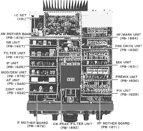
Yaesu FT-7B circuits, top view
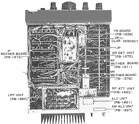
Yaesu FT-7B circuits, bottom view
FT-7B receiver circuit :
The signal from the antenna is fed through a low-pass filter consisting of L2701, C2701, and C2702, is switched through RL1, and is fed to the RF ATT UNIT (PB-1883). Here, 20 dB of attenuation may be placed in the antenna line by activating the front panel attenuator switch, which places R2101 - R2103 in the incoming signal path. The signal then passes through a tuning circuit consisting of T1921 - T1925 and VC1901, and is delivered to pin 9 of the RF/MARK UNIT (PB-1884).
The signal is applied to gate 1 of the RF amplifier, Q104 (3SK51-03), a dual-gate MOSFET. AGC voltage is applied to gate 2 of Q104 to control the gain of this stage, thus preventing overload in succeeding stages. The amplified signal is then fed through the passband tuning circuit to the MIXER UNIT (PB-1631). Buffer amplifier Q201, (2SC535A) is used to accomplish impedance matching between the RF amplifier and the diode mixer. The incoming signal is mixed by the diode mixer, consisting of D203 - D206 (1SS16 type), with the signal from the premix circuit. Schottky barrier diodes are used to secure high dynamic range with low noise characteristics.
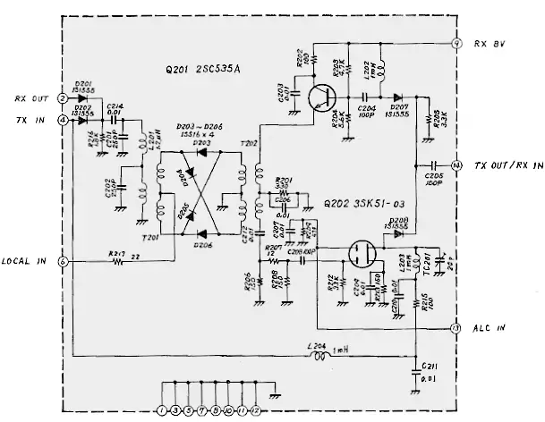
Yaesu FT-7B MIXER unit (PB-1631E) schematic diagram
The mixer produces a 9 MHz intermediate frequency (IF) at the output of T201. The IF signal is fed through a low pass filter consisting of L201, C201, and C202, passed through diode switch D201, and delivered to the FILTER UNIT (PB-1873). The IF signal is passed through a monolithic filter, XF301, and is amplified by IF amplifiers Q301 and Q302 (2 x 2SK19GR). Noise blanker diode D301 (1S1007) is controlled by Q303 (MPSA13) to eliminate noise pulses.
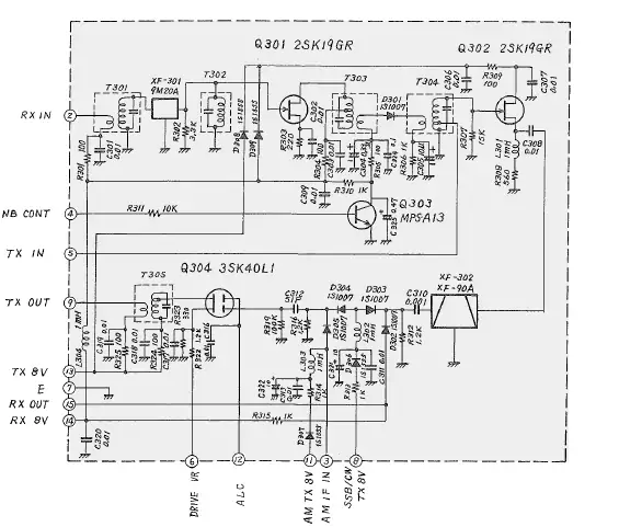
Yaesu FT-7B FILTER unit (PB-1873A) schematic diagram
The output from Q302 passes through a 6-pole crystal filter and diode switch D303 (1N60), and is fed to the IF UNIT (PB-1625). The IF signal is further amplified by Q401 and Q402 (2 x 3SK61-03). On SSB and CW, the amplified signal is fed to the ring demodulator, D509 - D512 (1S1007), also fed to the ring demodulator is the carrier signal from buffer amplifier Q503 (2SC372Y).
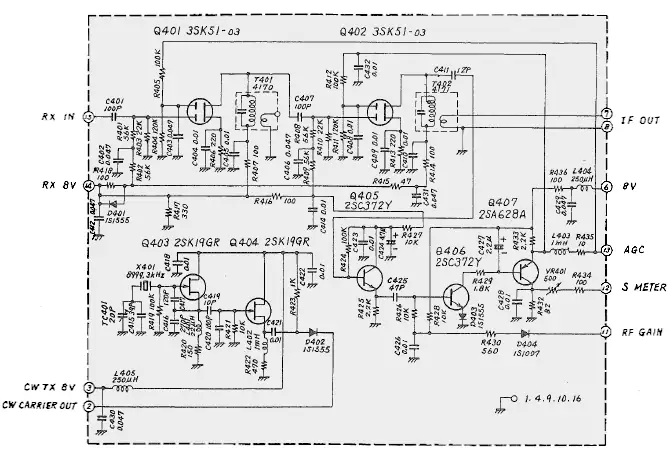
Yaesu FT-7B IF unit (PB-1625E) schematic diagram
An AM signal is amplified by Q2401 (2SK19GR), detected by AM detector D2403 - D2404 (1S1007), and the resulting audio signal is amplified by Q2402 (2SC372Y) and delivered to the AF UNIT. When the MODE switch is placed in the CW position, Q2301 (2SD636) causes Q2602 (MC14016B) to switch a highly selective audio peak filter into the circuit. Q2604 (MC1741) and associated shaping circuitry provide a bandwidth of approximately 80 Hz at 6 dB down, thus improving dramatically the system signal-to-noise ratio. VR2601 provides adjustment of the center frequency of the audio filter. The signal is then passed to the AF UNIT. On SSB and CW, the audio signal from the ring demodulator or audio filter, respectively, is amplified by Q602 (2SC1000GR) and Q603 (TA7205AP), to deliver 3 Watt of audio output to the speaker. On AM, the output from the AM DET UNIT is fed directly to Q603 for amplification.
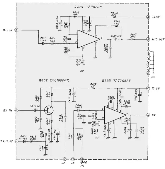
Yaesu FT-7B AF unit (PB-1648) schematic diagram
A portion of the 9 MHz IF signal is fed to pin 2 of the NB UNIT. When the NB/MARK switch is placed in the NB (noise blanker) position, the signal is amplified by Q801 (3SK51-03) and fed to the gate of noise blanker mixer Q802 (3SK51-03), where an 8545 kHz signal generated by Q805 (2SK19Y) is mixed with the incoming IF signal, producing a 455 kHz noise blanker IF. This IF signal is then amplified by Q803 (3SK51-03). When a carrier or noise-free modulated signal is received, the 455 kHz signal is rectified by D801 and D802 (1N60), and the voltage is used to charge C813. There is no discharge loop for C813, therefore a signal which exceeds the charged voltage established by the reference voltage on C813 will not pass through D801 and D802. Accordingly, there will be no voltage drop across R819, and Q804 (3SK51-03) will conduct as the gate voltage approaches zero, causing the drain to drop.
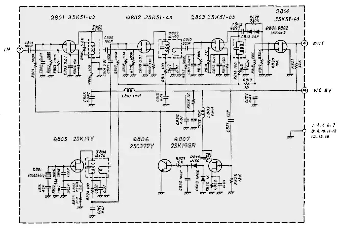
Yaesu FT-7B NB unit (PB-1627D) schematic diagram
The drain of Q804 is connected directly to the base of noise gate controller Q303 (MPSA13), located on the FILTER UNIT. The voltage drop of the drain will turn off Q303, causing a forward bias to D301. As D301 conducts, the signal will pass through the circuit. When impulse noise is received. which exceeds the charged reference voltage on C813, D801 and D802 will permit negative-going pulses to turn off Q804. Thus, Q303 will conduct and D301 will be biased to block the signal passage. The signal amplified by Q807 (2SK19GR) is rectified by D804 and D805 (2 x 1N60). The rectified DC voltage is amplified by amplifier Q806 (2SC372Y) and fed to the gates of Q801 and Q803 to control the gain of these stages.
The crystal controlled marker generator, Q101 (2SC372Y), located on the RF/MARK UNIT, generates a fundamental 12.8 MHz signal. The 12.8 MHz signal is fed through buffer amplifier Q102 (2SC372Y) to frequency divider Q103 (F4024PC), which produces a 100 kHz marker signal. The 100 kHz marker signal is fed through pin 4 and pin 9 to the receiver front end.
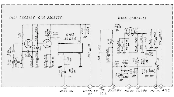
Yaesu FT-7B RF/MARKER unit (PB-1884B) schematic diagram
Speech input from the microphone jack J7 is fed through the MIC GAIN control VR3 to pin 2 of the AF UNIT for SSB. The speech signal is amplified by Q601 (TA7063P) and fed to the ring modulator, D501 - D504 (1S1007) in the MOD/DEM UNIT. The signal modulates the carrier signal delivered from Q503, and the resulting 9 MHz double sideband signal is amplified by Q501 (2SK19Y) and fed through diode switch D505 (1S1555) to the FILTER UNIT.
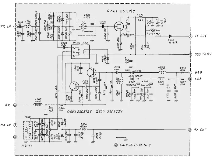
Yaesu FT-7B MOD/DEM unit (PB-1878A) schematic diagram
The signal is amplified by a buffer, Q302 (2SK19GR), and fed to crystal filter XF302 where the unwanted sideband is rejected. The 9 MHz SSB signal is then fed through diode switch D303 - D304 (2 x 1S1007) to Q304 (3SK40L1), and the amplified signal is fed to pin 4 of the MIXER UNIT. The 9 MHz SSB signal is heterodyned to the desired RF frequency by injection of the local signal supplied from the PREMIX UNIT. The RF output from the diode mixer is amplified by Q202 (3SK51-03) and fed through diode switch D208 (1S1555) and bandpass transformers T1906 - T1915 to the PRE DRIVE UNIT. The bandpass transformers are used on both transmit and receivem to provide extremely high selectivity.
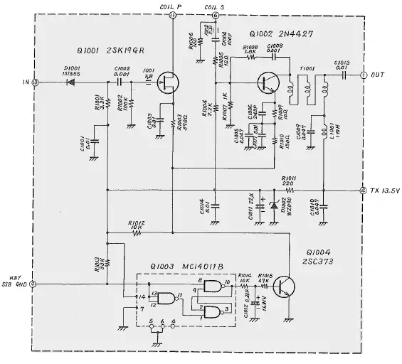
Yaesu FT-7B PRE DRIVE unit (PB-1632) schematic diagram
In the AM mode, the speech signal is amplified by Q2301 (2SC1000GR) and fed to the AM modulator, Q2302 (3SK59GR), where the speech signal modulates the 8999.3 MHz carrier signal generated by Q403 (2SK19GR) and delivered from Q404 (2SK19GR). The modulated signal is delivered to Q304, and from there its path is identical to that of the SSB signal. In the CW mode, the carrier signal from Q404 passes through XF302 and is fed to Q304. The tone oscillator, Q701 (2SC373), operates when the MODE switch is in the CW position. It consists of a phase shift oscillator operating at approximately 800 Hz. The tone output is activated by the keying circuit, and is coupled to Q702 (2SC372Y) for semi-break-in CW operation. The relay delay hold time is adjusted by VR702. The emitter voltage of Q1001 and Q1002 is controlled by keying switch transistor Q1004 (2SC373). A flip-flop circuit utilizing Q1003 (MC14011B) is employed to secure a perfectly-shaped waveform for CW transmission, free of clicks at any keying speed.
The RF signal on all modes is amplified by Q1001 (2SK19GR) and Q1002 (2N4427), and delivered to the POWER AMP UNIT. The signal is amplified by drivers Q2201 (2SC1589) and Q2202 (2SC2395), and the resulting output drives the push-pull power amplifier, consisting of Q2203 and Q2204 (2SC2099), producing a nominal power output of 50 Watt. The RF signal passes through the low-pass filter, as well as the CM coupler, and is delivered through antenna relay RL1 to the antenna. Q2205 (2SD235), as well as diodes D2203 - D2204 (2 x 10D10), provide bias compensation and thermal runaway protection for the final transistors.
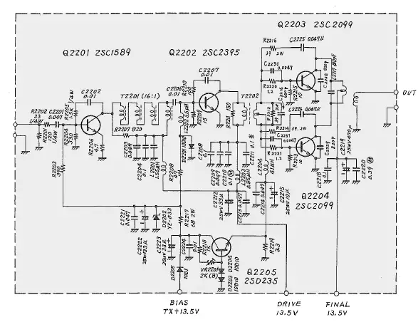
Yaesu FT-7B POWER AMP unit (PB-1879A) schematic diagram
T1501 detects the forward and reflected waves of the transmit signal. The forward wave is rectified by D1502 (1S1555), and the reflected wave by D1501 (1S1007), to generate ALC voltage. The ALC threshold level of the forward wave is set by VR1501. When there is an excessive amount of reflected power, the reflected wave is rectified by D1501, producing minus voltage on the ALC line. The ALC voltage reduces the gain of Q304 to prevent overloading or distortion.
FT-7B VFO circuit :
A modified Colpitts type oscillator is used to generate a 5.0 - 5.5 MHz signal to produce a stable 500 kHz tuning range. The frequency is varied by VC1201, which is geared to a precision-built dial tuning mechanism. Varactor diode D1201 (1S2236) is in series with C1207, and the combination is in parallel with VC1201. By activating the clarifier switch, the clarifier control shifts the receiver ±3 kHz.
The VFO output signal is fed through amplifier/buffer stages Q1202 (2SK19GR) and Q1203 (2SC372Y), the low-pass filter, and diode switch D1202 (1S1555) to the PREMIX UNIT. In addition to normal VFO operation, one crystal controlled channel per band may be used. Crystal oscillator Q1101 (2SC372Y) is followed by buffer amplifier Q1102 (2SC372Y), and its output is fed through the low-pass filter and diode switch D1901 (1S1555) to the PREMIX UNIT. Trimmer capacitors TC1101 - TC1105 are used for fine adjustment of the crystal frequency.
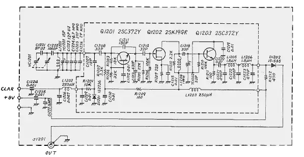
Yaesu FT-7B VFO unit (PB-1440) schematic diagram
Crystal oscillator Q1901 (JF1033) produces a heterodyne signal selected by the band switch. The signal is fed to the double balanced mixer Q901 (MC1496G) in the PREMIX UNIT, where the signal is mixed with the VFO signal. The output from the mixer is fed through bandpass transformers T1902 - T1905, to the broadband amplifier Q902 (2SK19GR), Q903 (2SC784R), and Q904 (2N4427). The premix output signal is then applied to the diode mixer in the MIX UNIT. A portion of the premix signal is fed through buffer Q1 (2SC372Y) to the EXT DIS jack, for use with the optional YC-7B digital frequency display unit.
FT-7B crystal circuits :
The carrier oscillator Q502 (2SC372Y) is followed by buffer amplifier Q503 (2SC372Y). Oscillation is at either 8998.5 kHz (40 - 10 meters LSB, 80 meters USB) Via X501, or 9001.5 kHz (40 - 10 meters USB, 80 meters LSB) via X502, depending on the mode of operation. Crystal selection is made by diode switches D507 and D508 (2 x 1S1555). The carrier is then fed through relay RL501 to the ring modulator/ demodulator. The LSB crystal is used for CW reception on all bands. For CW transmission, the oscillator in the IF UNIT oscillates with X401.
FT-7B price
We have collected for your convenience the Yaesu FT7B sale price (US Dollar) and its trend over time. Useful to guarantee a cheaper purchase of this radio and to put it for sale in the second-hand market. Of course offers, accessories, warranty terms and conditions can lead to different figures.
|
|
|
|
|
USD 294.00 (250EUR) |
2021-jan |
Second Hand Good condition overall |
|
USD 212.00 (187EUR) |
2019-nov |
Second Hand Comes with DC power cord, hand microphone, car mounting bracket |
| USD 215.00 | 2012-jan |
Second Hand Without the original microphone. Comes with original owner's manual |
FT-7B review
| Clemens, DL2GAN | August-1 2023 |
I use this nice old radio (FT-7b) as a backup transceiver in my home QTH or as main TRX in portable locations, such as campsites or holiday apartments. This radio perform still strong, I always get good modulation reports for SSB operation. The TRX performs well on CW, the CW audio filter is very narrow which is good for reception in crowded bands. Lately I had a QSO in AM mode on 10 meters, 29.050 MHz, which was surprisingly good and stable (Central Poland to Sicily Island). Audio bandwidth for AM reception is limited due to the fact, that the SSB filter 2.7 kHz is used for AM reception. I got this radio second hand in 1995.
[End post]
| Yaesu liefhebber | December-31 2022 |
I have owned the yaesu FT7-B for a long time. Good Tranceiver, where you have to be careful with the transmitter output stage. Yeasu supplies it as a 50W output stage, but in reality it can only supply 40W PEP. Good antenna tuning is therefore important, because the output stage is underdimensioned, and defective output stages were notorious for these transceivers. The receiver sensitivity was very good, especially on the 10m band, but that high sensitivity was at the expense of the strong signal behavior, especially on the 80 and 40m band. It is therefore not recommended to connect antennas that are too large. But in general it was and is a fine transceiver that can still deliver results in 2022.
[End post]
Your opinion on merits, defects, experiences, with this radio set is welcome. Write your review, after a technical evaluation by our staff if found suitable will be published on this page. We thank you for your precious contribution.
